- 您现在的位置:买卖IC网 > Sheet目录3862 > PIC16F916-I/ML (Microchip Technology)IC PIC MCU FLASH 8KX14 28QFN
211
8018P–AVR–08/10
ATmega169P
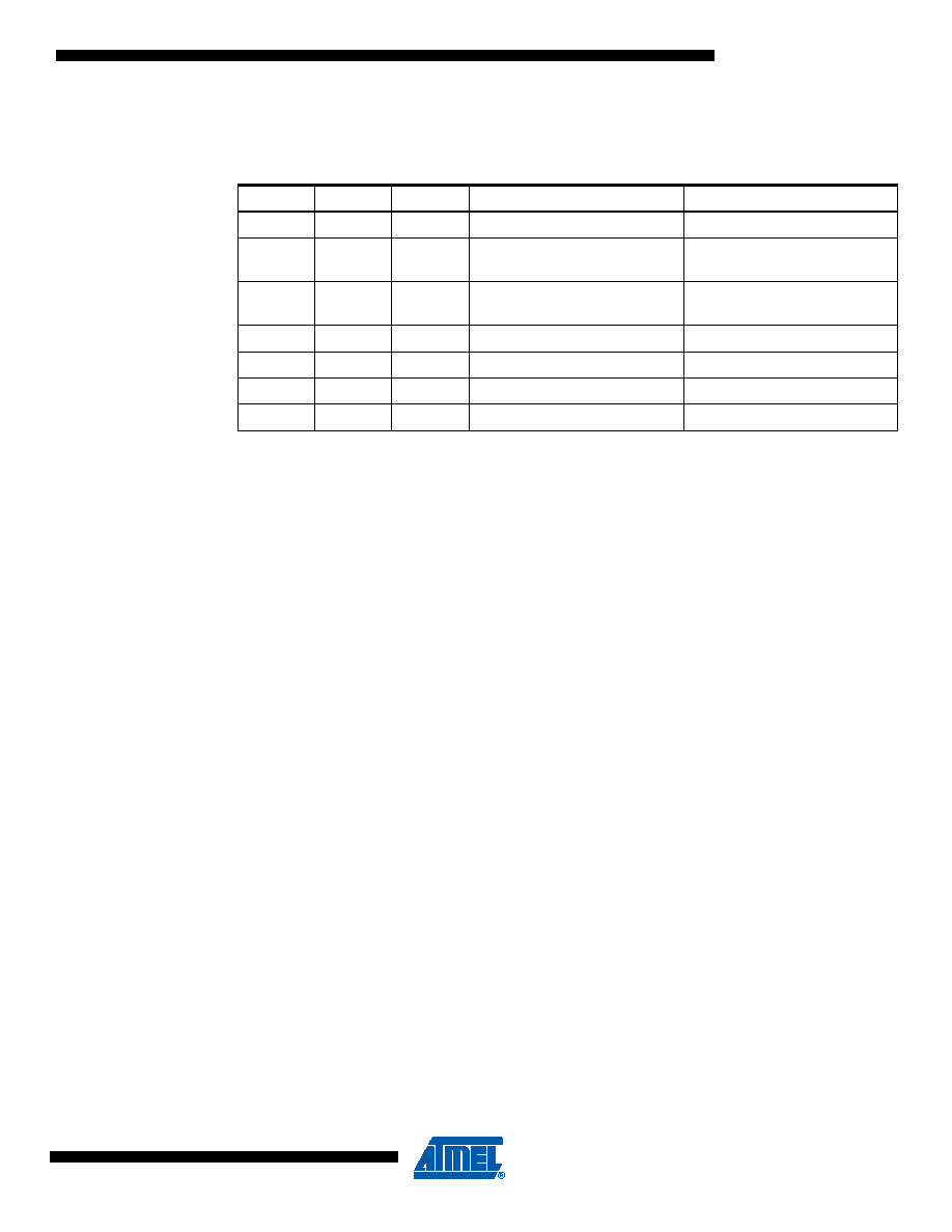
Table 20-2 shows the relationship between the USICS1:0 and USICLK setting and clock source
used for the Shift Register and the 4-bit counter.
Bit 1 – USICLK: Clock Strobe
Writing a one to this bit location strobes the Shift Register to shift one step and the counter to
increment by one, provided that the USICS1..0 bits are set to zero and by doing so the software
clock strobe option is selected. The output will change immediately when the clock strobe is exe-
cuted, that is, in the same instruction cycle. The value shifted into the Shift Register is sampled
the previous instruction cycle. The bit will be read as zero.
When an external clock source is selected (USICS1 = 1), the USICLK function is changed from
a clock strobe to a Clock Select Register. Setting the USICLK bit in this case will select the
USITC strobe bit as clock source for the 4-bit counter (see Table 20-2).
Bit 0 – USITC: Toggle Clock Port Pin
Writing a one to this bit location toggles the USCK/SCL value either from 0 to 1, or from 1 to 0.
The toggling is independent of the setting in the Data Direction Register, but if the PORT value is
to be shown on the pin the DDRE4 must be set as output (to one). This feature allows easy clock
generation when implementing master devices. The bit will be read as zero.
When an external clock source is selected (USICS1 = 1) and the USICLK bit is set to one, writ-
ing to the USITC strobe bit will directly clock the 4-bit counter. This allows an early detection of
when the transfer is done when operating as a master device.
Table 20-2.
Relations between the USICS1:0 and USICLK Setting
USICS1
USICS0
USICLK
Shift Register Clock Source
4-bit Counter Clock Source
0
No Clock
00
1
Software clock strobe
(USICLK)
Software clock strobe
(USICLK)
01X
Timer/Counter0 Compare
Match
Timer/Counter0 Compare
Match
1
0
External, positive edge
External, both edges
1
0
External, negative edge
External, both edges
1
0
1
External, positive edge
Software clock strobe (USITC)
1
External, negative edge
Software clock strobe (USITC)
发布紧急采购,3分钟左右您将得到回复。
相关PDF资料
PIC16C716-20I/P
IC MCU OTP 2KX14 A/D PWM 18DIP
PIC18F26K80-I/SO
MCU PIC 64KB FLASH 28SOIC
PIC18F26J13-I/SS
IC PIC MCU 64KB FLASH 28SSOP
SFW27R-1STE1
SFW27R-1STE1-FFC/FPC CONN
PIC18F66J15-I/PT
IC PIC MCU FLASH 48KX16 64TQFP
PIC24FV32KA302-I/SO
MCU 32KB FLASH 2KB RAM 28-SOIC
PIC24HJ64GP204-I/ML
IC PIC MCU FLASH 64K 44-QFN
SFW27R-2STE1
SFW27R-2STE1-FFC/FPC CONN
相关代理商/技术参数
PIC16F916-I/SO
功能描述:8位微控制器 -MCU 14KB FL 352R 25 I/O RoHS:否 制造商:Silicon Labs 核心:8051 处理器系列:C8051F39x 数据总线宽度:8 bit 最大时钟频率:50 MHz 程序存储器大小:16 KB 数据 RAM 大小:1 KB 片上 ADC:Yes 工作电源电压:1.8 V to 3.6 V 工作温度范围:- 40 C to + 105 C 封装 / 箱体:QFN-20 安装风格:SMD/SMT
PIC16F916-I/SO
制造商:Microchip Technology Inc 功能描述:8 Bit Microcontroller Clock Speed:20MHz
PIC16F916-I/SOG
制造商:Microchip Technology Inc 功能描述:8BIT MCU FLASH SMD 16F916 SOIC28
PIC16F916-I/SP
功能描述:8位微控制器 -MCU 14KB FL 352R 25 I/O RoHS:否 制造商:Silicon Labs 核心:8051 处理器系列:C8051F39x 数据总线宽度:8 bit 最大时钟频率:50 MHz 程序存储器大小:16 KB 数据 RAM 大小:1 KB 片上 ADC:Yes 工作电源电压:1.8 V to 3.6 V 工作温度范围:- 40 C to + 105 C 封装 / 箱体:QFN-20 安装风格:SMD/SMT
PIC16F916-I/SP
制造商:Microchip Technology Inc 功能描述:8 Bit Microcontroller Clock Speed:20MHz
PIC16F916-I/SS
功能描述:8位微控制器 -MCU 14KB FL 352R 25 I/O RoHS:否 制造商:Silicon Labs 核心:8051 处理器系列:C8051F39x 数据总线宽度:8 bit 最大时钟频率:50 MHz 程序存储器大小:16 KB 数据 RAM 大小:1 KB 片上 ADC:Yes 工作电源电压:1.8 V to 3.6 V 工作温度范围:- 40 C to + 105 C 封装 / 箱体:QFN-20 安装风格:SMD/SMT
PIC16F916-I/SS
制造商:Microchip Technology Inc 功能描述:8-Bit Microcontroller IC
PIC16F916T-E/MLC02
制造商:Microchip Technology Inc 功能描述: